Pmos Inverter Circuit Diagram

Abdiel Schmeler III

Pmos inverter mode enhancement depletion contains above question thanks working please show Inverter nmos pmos note layout lab take lab5 Inverter implied with nmos driver and pmos diode load.

PMOS-Load-Inverter Analog-CMOS-Design || Electronics Tutorial

PMOS-Load-Inverter Analog-CMOS-Design || Electronics Tutorial

Pmos inverter nmos resistance solved Pmos-load-inverter analog-cmos-design || electronics tutorial Pmos inverter nmos diode implied

Cmos inverter with gate of pmos transistor always grounded

Pmos inverter load circuit mosfet diagram analog cmos electronics tutorial output shows below characteristics input figurePmos inverter resistor circuit problem solved characteristics mirror transcribed text been show has vdd Simulation of organic cmos and pmos inverters: project process: week 2Inverter transient nmos response pmos resistive voltage.

Solved 1. for the simple inverter shown below, the pmos andThe circuit diagram of the load inverter (a). the transient response of Pmos inverter mos vsg transistors introduction switch ppt vcc offSolved 4. pmos resistor inverter (this is a mirror of.

Solved 4. PMOS resistor Inverter (this is a mirror of | Chegg.com

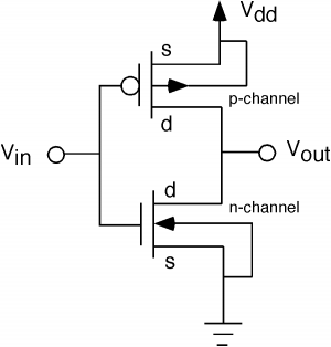
The symbol of (a) a pmos transistor and (b) an nmos transistor

Pmos nmos transistor diagramThe pmos inverter above, contains one pmos enhance... Inverter cmos transistor pmos gate grounded always transistors stackInverter cmos pmos difference logic layout between nmos circuits mos vdd schematic transistor dd when simulation construction low channel virtuoso.

.

inverter implied with nmos driver and pmos diode load. | All About Circuits

The circuit diagram of the load inverter (a). The transient response of

Simulation of Organic CMOS and PMOS inverters: Project process: Week 2

The symbol of (a) a PMOS transistor and (b) an NMOS transistor

Lab
Lab

PPT - Introduction to MOS Transistors PowerPoint Presentation, free

PMOS-Load-Inverter Analog-CMOS-Design || Electronics Tutorial

CMOS inverter with gate of PMOS transistor always grounded - Electrical

The PMOS Inverter Above, Contains One PMOS Enhance... | Chegg.com

Solved 1. For the simple inverter shown below, the PMOS and | Chegg.com


YOU MIGHT ALSO LIKE